
When and why to use multilayer PCB
In today’s world, where electronics are becoming increasingly powerful and compact, it's no longer sufficient to place components on just one or two PCB layers. The more complex the design, the more demanding the requirements—and that’s where multilayer PCBs come into play.
What are multilayer boards and why do they matter?
Unlike standard single - or double-layer boards, multilayer PCBs consist of three or more layers of conductive pathways, separated by insulating material (typically FR4). These layers are compressed into a single unit through lamination, forming a sandwich-like structure.
The result? The ability to route hundreds of signal paths in a compact space, significantly improved electrical performance, and much higher reliability—even under demanding operating conditions.
How does it work?
Multilayer PCBs are not just about stacking more layers. Their design requires a deeper understanding of the stack-up—the order and function of each layer.
Today, PCBs with 32 or more layers are common, and the technologies to manufacture them are highly advanced. In theory, it's possible to create PCBs with 100+ layers. Smartphones may have up to 12 layers, depending on the complexity of their applications.
Alternating layers are compressed at high temperature and pressure to eliminate any trapped air. This encapsulates the conductive layers in resin, ensuring a safe and reliable result.
This arrangement is deliberate. Ground and power layers act as shields, protecting signal layers from electromagnetic interference (EMI) and ensuring stable return paths for current.
Multilayer PCB - typical layer stack-up example
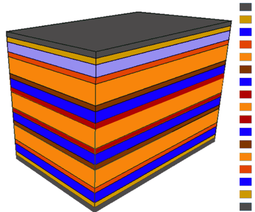
Solder mask (top)
Copper layer
Prepreg (adhesive and dielectric)
Power layer
Core
Ground layer
Prepreg
High-speed signal layer
Core
High-speed signal layer
Prepreg
Ground layer
Core
Power layer
Prepreg
Copper layer
Solder mask (bottom)
Layer connection: Vias
- Through-hole vias pass through the entire board.
- Blind vias connect the surface with an internal layer.
- Buried vias connect only internal layers and are invisible from the outside.
- Microvias are extremely small vias used in HDI (High-Density Interconnect) boards, enabling very high routing density.
What happens if the layers are not properly designed?
A poorly designed stack-up can severely impact the functionality and reliability of the entire device. Issues such as incorrect placement of power and ground layers, lack of symmetry, or absence of controlled impedance can lead to:
- Degraded signal integrity – longer return paths cause more interference, reflections, and signal distortion, especially at high frequencies.
- Increased electromagnetic emissions (EMI) – improper shielding and current routing lead to more interference in surrounding circuits and even outside the board.
- Mechanical instability – asymmetrical stack-ups introduce internal stresses, causing warping or even board cracking during soldering.
- Reduced lifespan and reliability – improper layering increases the risk of delamination or via failure during thermal cycling.
That's why proper layer design is essential from the very start—not only for electrical performance, but also for mechanical and manufacturing robustness.
Benefits of multilayer PCBs
1. Electrical Performance - A well-designed multilayer PCB improves signal integrity significantly. Dedicated ground layers provide short and stable return paths, minimizing noise and reflections—essential for high-frequency data transmission.
2. Electromagnetic Compatibility (EMC) - Good shielding and proper layer arrangement lead to lower EMI. For comparison: a four-layer board can have emissions up to 15 dB lower than a similar two-layer board.
3. Compact Design - More layers mean fewer traces need to be routed on the surface, allowing smaller device sizes—key for wearables, drones, and medical devices.
4. Better Thermal Management - More layers mean more ways to dissipate heat—using copper pours or thermal vias.
When do you really need a multilayer PCB?
Multilayer PCBs are worth considering when:
- You have a complex circuit with high signal density
- You need stable signal integrity at high frequencies
- Your design has strict EMC requirements
- You need to save space (e.g., in mobile, modular, or embedded systems)
- You're working with high-speed buses (DDR, USB 3.0, etc.)

The evolution of multilayer PCBs
Latest innovations from Japan
Manufacturing multilayer PCB is among the most energy- and material-intensive processes in the electronics industry. It traditionally involves full-substrate copper plating, repeated etching, drilling, and lamination—using aggressive chemicals and producing significant material waste.
However, Japanese company Elephantech has completely reimagined this process and offers a breakthrough solution: inkjet printing of copper directly onto the base material.
How does it work?
The SustainaCircuits™ technology uses an inkjet method to precisely print copper traces according to the design—no full-surface plating or masking required.
First, a catalytic ink is printed onto an FR4 substrate with precise geometry. This ink is then activated and selectively plated with copper only where needed using localized electroplating. This scalable approach also supports multilayer boards, with vias printed and filled with copper as well.
Key advantages of the new Ttechnology
- 70–80% Copper Savings
Since copper is applied only where needed, there's no waste from etching, and recycling is easier. - No Full-Surface Plating = Less Chemistry
Traditional processes use acids, chrome baths, and harsh reagents. SustainaCircuits™ drastically reduces chemical usage. - Supports 4–8 Layer Designs
With additive layers and precise alignment, this method allows for complex multilayer designs, including functional vias. - Electroplated Tracks Up to 100 µm Thick
The process allows thickened traces for higher current loads and lower resistance. - Faster Manufacturing with Lower Environmental Impact
By eliminating steps like etching, lamination, and repeated drilling, the process becomes significantly faster and greener.
Commercial stage and early applications
In April 2025, Elephantech officially announced that its SustainaCircuits™ platform is available to selected industrial partners.
One of the first to adopt it was LITE ON, using the technology for custom production of multilayer modules.
However, a major breakthrough came from the consumer electronics sector: Logitech revealed it now uses boards made with this method in mass-produced MX Vertical mice.
This means the technology has moved beyond the lab and into real-world production—a rare milestone for new PCB fabrication methods.
A sustainable future for multilayer PCB?
With material savings, lower chemical usage, and shorter production cycles, inkjet-printed copper represents a highly promising future for PCB manufacturing. In an era of increasing focus on eco-design, circular economy, and carbon neutrality, this technology is a strong candidate for wider adoption—especially where high integration and sustainability are both essential (e.g., medical devices, wearables, IoT).
Sources:
- LITE-ON Technology Corporation (2025) Sustainable electronics and additive PCB manufacturing roadmap. Taipei: LITE-ON Group R&D Whitepaper.
- Logitech International S.A. (2025) Environmental Impact Report: Component Innovations in Consumer Electronics. Lausanne: Logitech Sustainability Division.
- IEEE (2024) ‘Additive manufacturing in PCB fabrication: emerging trends’, IEEE Transactions on Components, Packaging and Manufacturing Technology, 14(3), pp. 312–320. doi:10.1109/TCPMT.2024.1234567.
- Elephantech Inc. (2024) SustainaCircuits™ – mass production of multilayer printed circuit boards by inkjet printing. [Online] Available: https://elephantech.com/en/news/press_release_20250422 [Accessed 14 Jul. 2025].
- Yamada, K., Tanaka, T., and Sato, M. (2023) ‘Development of multilayer PCBs using inkjet-printed copper patterning’, Journal of Electronic Materials, 52(9), pp. 4256–4264. doi:10.1007/s11664-023-10573-2.
Would you like to know more about this topic?
Get in touch with our experts.
What are multilayer boards and why do they matter?
Multilayer PCB - typical layer stack-up example
What happens if the layers are not properly designed?
When do you really need a multilayer PCB?
The evolution of multilayer PCBs
Key advantages of the new Ttechnology