Skip to content

Top 10 Tips for Successful PCB Fabrication Techniques?

In the fast-evolving world of PCB fabrication, staying ahead of the curve is essential for success. Experts like Dr. Emily Zhao emphasize the importance of mastering techniques in this industry. She states, “Precision and innovation determine the future of PCB fabrication.” This quote highlights the critical role of quality and creativity in producing high-performance PCBs.

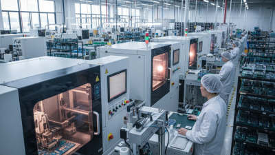
PCB fabrication involves a series of intricate processes. Each step, from design to assembly, must be meticulously managed. Common mistakes can lead to costly delays. For example, overlooking design rule checks could compromise the product’s integrity. Innovation and quality control are vital in this field. The demands on PCB fabrication require professionals to constantly refine their skills and techniques.

Despite advancements in technology, challenges persist. Many fabricators struggle with scaling production without sacrificing quality. Each project presents unique hurdles that require thoughtful solutions. Reflecting on past experiences can reveal important lessons. Continuous improvement is key to mastering PCB fabrication and achieving industry excellence.

Top 10 Tips for Successful PCB Fabrication Techniques?

Understanding PCB Fabrication Materials: Choosing the Right Substrate

Top 10 Tips for Successful PCB Fabrication Techniques?

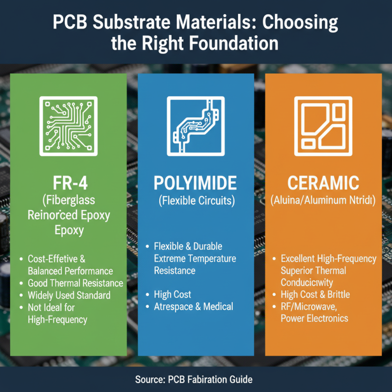
Choosing the right substrate is crucial for PCB fabrication. Each material has distinct properties affecting performance. Common substrates include FR-4, polyimide, and ceramic. FR-4 is widely used due to its balance of cost and performance. It handles heat well but may not suit high-frequency applications. Polyimide is flexible and can endure extreme temperatures. However, it tends to be more expensive.

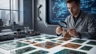
Ceramic substrates offer excellent insulation and thermal conductivity. They are ideal for high-power applications but can be brittle. When selecting a substrate, consider your product's environment. Will it experience moisture or mechanical stress? Such factors can influence material choice. It's also important to match the substrate with the desired circuit design. Sometimes, engineers overlook these details, leading to suboptimal performance.

Reflecting on the process is vital. Engineers need to weigh the pros and cons of different substrates. Choosing the wrong material can result in failures during testing. Additionally, understanding each substrate’s limitations can help avoid design flaws. Review previous projects to identify mistakes. Continuous learning is essential for improvement.

Essential Design Practices for Optimizing PCB Layout Efficiency

When optimizing PCB layout efficiency, attention to design practices is crucial. Recent studies indicate that a well-optimized layout can reduce manufacturing costs by up to 30%. Simple practices yield significant results. For instance, maintaining proper trace width helps avoid overheating and signal integrity issues. A common error is ignoring minuscule adjustments that can lead to costly failures.

Via proper spacing and layout, designers can enhance signal flow. The ideal trace-to-trace spacing is often less than 0.5 mm. Unfortunately, many overlook these measurements. This oversight can lead to increased electromagnetic interference. Keeping component placement efficient minimizes routing complexity. It’s essential to think critically about every placement. Effectively utilizing available space cuts manufacturing lead times.

Testing is essential, yet often neglected. Pre-fabrication verification ensures design accuracy. According to industry reports, about 20% of PCBs fail due to design flaws. Regular testing can help identify risks. Adopting design rules can guide engineers toward better practices. Small refinements in the design stage can yield profound impacts on overall efficiency. The focus must remain on both functionality and manufacturability.

Quality Control Measures: Ensuring Accuracy in PCB Fabrication

Quality control is essential in PCB fabrication. Accurate measurements ensure that each board meets the design specifications. A study from IPC states that 60% of defects arise from process variations. These variations can lead to significant failures in the final product.

Implementing strict quality control measures can significantly reduce these issues. For instance, automated visual inspection systems can catch flaws earlier. According to a recent industry report, automation can decrease defect rates by up to 30%. However, human oversight is still crucial. Relying solely on machines may lead to oversight of nuanced defects.

Regular audits and testing are important. Random sampling of finished PCBs helps identify trends in quality. The ongoing challenge is keeping up with new technologies. As fabrication processes evolve, adapting quality measures is vital. Mistakes in the past often arise from outdated methodologies. This highlights the need for continuous improvement in quality controls.

Latest Trends in PCB Fabrication Technologies and Techniques

The landscape of PCB fabrication is evolving rapidly. Recent industry reports indicate a projected growth of 4.2% annually, driven by innovations in materials and manufacturing processes. Today's techniques emphasize automation and precision, reducing human error while improving product quality.

Incorporating advanced technologies like artificial intelligence is also becoming common. AI helps in design validation and error detection. This trend allows companies to cut down on production time and enhance efficiency. Furthermore, the adoption of eco-friendly materials is on the rise, with many manufacturers using biodegradable laminates to meet environmental standards.

Tip: Regularly update your knowledge. Attend industry conferences or webinars to stay informed.

Another key trend is the shift towards miniaturization. As devices become smaller, PCBs must adapt. Fine-pitch components and complex multilayer boards are now standard. Manufacturers are challenged to maintain quality while achieving these micro-level specifications.

Tip: Invest in quality control. Proper inspection procedures can catch defects early.

Being agile and adaptable is essential in this competitive environment. Companies need to rethink traditional practices to stay relevant and meet market demands. Embracing these changing dynamics can lead to more successful PCB fabrication.

Top 10 Tips for Successful PCB Fabrication Techniques

Tip Number Technique Description Latest Trend
1 Design Precision Ensure high accuracy in PCB layout to avoid errors. AI-based Design Tools
2 Quality Materials Use high-quality substrates to enhance performance. Eco-friendly Materials
3 Advanced Prototyping Rapid prototyping to test designs quickly. 3D Printing
4 Layer Stack-up Optimize layer arrangement for signal integrity. Multi-layer PCBs
5 Thermal Management Implement heat dissipation strategies early. Thermal Simulation Software
6 Design for Manufacturability (DFM) Adhere to manufacturing guidelines to minimize defects. Automated DFM Tools
7 Testing Protocols Implement rigorous testing processes to ensure reliability. Automated Testing Systems
8 Supply Chain Management Optimize sourcing to avoid delays in production. Blockchain for Transparency
9 Supply Chain Diversification Avoid reliance on single suppliers to mitigate risks. Global Supplier Network
10 Environmentally Friendly Processes Adopt green practices in PCB manufacturing. Sustainable Materials and Waste Reduction

Cost Management Strategies for Successful PCB Production and Sourcing

Managing costs in PCB production can be challenging. Many factors influence expenses, such as material choices and manufacturing processes. It's vital to analyze each cost component. For example, premium materials may boost quality but will raise costs. Striking a balance is key.

Outsourcing some elements can help manage costs. However, quality control becomes a concern. Ensuring the supplier meets your standards is crucial. Miscommunication can lead to mistakes, costing more in the long run. Setting clear guidelines can help minimize these risks.

Design is another critical area. A well-optimized PCB design reduces material waste. Using simulation tools can save time and resources. Yet, it can be difficult to predict every possible issue. Regular reviews can lead to better designs and lower costs. Keep refining your processes to achieve success.