What is PCB Prototyping and Why is it Important?
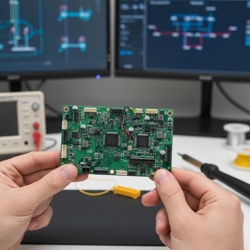
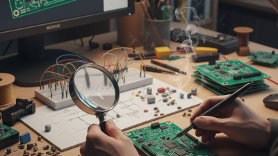
PCB prototyping is a crucial step in the development of electronic devices. It allows engineers to test and validate their designs quickly. By creating a physical model, they can identify issues early in the process. This prevents costly mistakes later on.
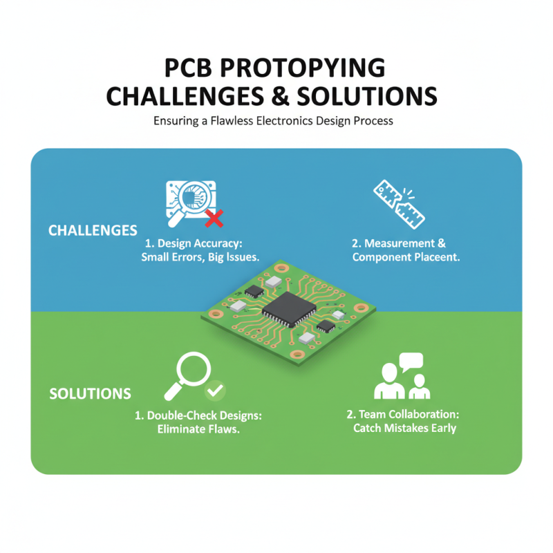
In today's fast-paced tech world, having a reliable PCB prototype is vital. It bridges the gap between concepts and real-world applications. However, many still overlook its importance. Rushing through the prototyping phase can lead to flawed products. Consider the potential consequences of a failed prototype.
Mistakes during PCB prototyping can impact the entire project timeline. Engineers should invest time into this stage. Quality and precision in prototypes can lead to successful product launches. Embracing a thorough approach can save resources in the long run.
Understanding PCB Prototyping: Definition and Overview
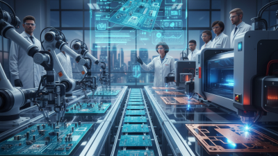
PCB prototyping is a critical process in electronics design. It involves creating a scaled-down version of a printed circuit board (PCB). This prototype helps engineers test the design before full-scale production. Prototyping allows for early detection of design flaws, which can save both time and resources.
One tip for effective prototyping is to focus on key components. Identify which parts of your design are most likely to benefit from testing. This can streamline the process and highlight areas that need improvement. Remember, not every detail must be perfect at this stage.
Another useful tip is to gather feedback early. Share your prototype with peers or potential users. Their insights can reveal overlooked issues. Engaging others in the testing phase fosters collaboration and enhances the design. Be open to criticism; it’s a step toward refinement. The prototyping process is iterative, making adjustments based on feedback essential for success.
Related Posts
-
What is PCB Fabrication and How Does it Impact Your Electronics Projects
-
Why Understanding PCB Production is Essential for Modern Electronics
-
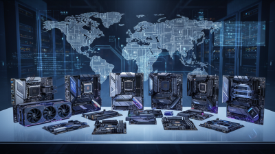
Top 10 PC Boards for Optimal Performance in 2023
-
How to Start PCB Prototyping for Your Electronics Projects?
-
Top 10 PCB Fast Manufacturing Techniques to Improve Efficiency?
-
Why Printable Circuit Boards are Revolutionizing Modern Electronics Design