Skip to content

How to Master Printed Circuit Board Manufacturing Techniques and Best Practices?

Mastering printed circuit board manufacturing techniques is crucial in today’s tech-driven world. Experts like Dr. Mark Thompson from TechPCB emphasize, “Precision in PCB design and manufacturing can define the success of an electronic product.” This highlights the necessity of understanding and mastering the processes involved.

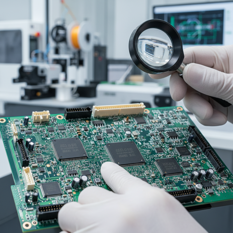
In printed circuit board manufacturing, attention to detail is vital. Each phase, from design to assembly, requires skilled execution. A small error can lead to significant failures. Learning from mistakes and acknowledging flaws in methods helps improve quality. Continuous improvement is essential in achieving excellence.

Developing expertise in printed circuit board manufacturing requires dedication. It’s not just about following steps; it's about understanding the nuances. Engaging with experienced professionals can lead to better practices. The manufacturing landscape is always evolving, demanding adaptability and a proactive approach.

How to Master Printed Circuit Board Manufacturing Techniques and Best Practices?

Understanding the Basics of Printed Circuit Board Manufacturing

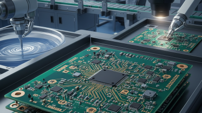
Printed circuit board (PCB) manufacturing is a complex process that involves various techniques and practices. Understanding these basics can significantly improve the quality of PCBs. The journey begins with material selection. Choosing the right substrates and conductors is crucial. Copper is a common choice for conducting layers, while FR-4 is widely used for substrates.

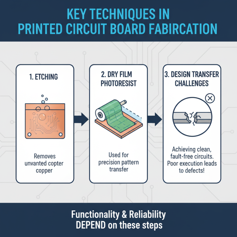
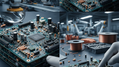
The manufacturing process typically includes designing the schematic and layout using specialized software. Even minor errors can lead to circuit failures. Hence, attention to detail is essential. Fabrication processes, such as etching and drilling, require precision. These steps transform a simple board into a functioning electrical pathway.

It's essential to be aware of potential mistakes. Over or under-etching can compromise the integrity of a PCB. Also, the quality of soldering techniques affects durability. Inadequate solder joints can lead to operational issues. Continuous learning and adaptation are vital in mastering PCB manufacturing techniques. Analyzing past projects helps identify areas for improvement, fostering expertise in the field.

PCB Manufacturing Techniques: Efficiency and Quality Comparison

Key Techniques in Printed Circuit Board Fabrication

How to Master Printed Circuit Board Manufacturing Techniques and Best Practices?

Mastering printed circuit board (PCB) fabrication requires understanding key techniques. These techniques influence both functionality and reliability. One crucial method is etching, which removes unwanted copper from the board. Dry film photoresist is commonly used for precision. The challenge lies in achieving a clean transfer of designs during this step. A poorly executed etch can lead to faults that are difficult to trace.

Another vital aspect is drilling. High-speed machines are employed for accuracy. The choice of drill bits influences hole quality. Oversized holes can create issues with component fit. It’s essential to calibrate equipment regularly. The gap between design and execution is where mistakes often occur. Regular reviews during the process can save time and resources.

Lastly, surface finish processes protect circuits. They provide solderability and improve durability. Common finishes include HASL and ENIG, each with pros and cons. Knowing which finish to use can significantly impact board performance. However, some manufacturers overlook this step. The result may affect longevity and quality assurance. Achieving excellence in PCB fabrication involves constant learning and adjusting techniques.

Best Practices for Design and Layout of PCBs

Designing and laying out printed circuit boards (PCBs) is a critical step in electronics manufacturing. A well-designed PCB can significantly enhance the performance and reliability of an electronic device. However, many designers face challenges during this process. Understanding best practices is essential for achieving optimal results.

One of the key tips in PCB layout is to ensure proper component placement. Place high-frequency components close to each other to reduce signal loss. Additionally, maintain appropriate spacing between traces to avoid crosstalk. This practice not only improves performance but also simplifies manufacturing.

Another important aspect is grounding. A solid ground plane can reduce noise and improve signal integrity. Make sure to connect all grounds effectively. Use vias judiciously to avoid excessive inductance. Some designers underestimate the importance of via placement, which can lead to significant performance issues.

In summary, mastering PCB design involves attention to detail and careful planning. Evaluate your layouts regularly and seek feedback from peers. Continuous improvement is crucial, as even small adjustments can yield significant benefits.

Quality Control Measures in PCB Manufacturing Processes

Quality control in printed circuit board (PCB) manufacturing is vital for ensuring functionality and reliability. Effective measures include visual inspections, automated optical inspection (AOI), and electrical testing. These methods help to identify defects early, reducing costs and production time.

Despite advancements, challenges persist. Some defects may go undetected despite thorough testing. For instance, micro-cracks within layers might escape visual and electrical checks. Implementing a more comprehensive approach, like using x-ray inspection, could mitigate this issue. Regular audits of the quality control process can reveal areas for improvement.

Establishing a culture of quality is essential. Training staff on the significance of quality measures fosters a proactive mindset. Yet, it's crucial to understand that human error can occur. Continuous learning and feedback loops can enhance the overall quality control process. Emphasizing precision and attention to detail establishes reliability in the end product.

Innovations and Future Trends in PCB Manufacturing Techniques

In the ever-evolving landscape of printed circuit board (PCB) manufacturing, innovation is key. Today, trends like flexible circuits and multilayer designs are gaining traction. These technologies allow for more compact and efficient electronic devices. As manufacturers embrace these advancements, understanding their implications becomes crucial.

Tips for exploring this evolving field: Stay updated on the latest materials. Look for trends in sustainability and recycled materials. This not only benefits the planet but offers new opportunities for cost-effective solutions.

Another trend to watch is automation. Automated processes can optimize production time and reduce errors. By integrating advanced software, manufacturers can enhance design accuracy. However, dependence on automation may overlook niche innovations that human intuition can address. Balancing these approaches is essential for future success.

Keep an eye on the rise of additive manufacturing. This method fosters creativity and reduces waste. It challenges traditional PCB methods while opening up new possibilities for customization. Yet, the technology is still maturing and has a learning curve that should not be underestimated. Embrace experimentation, but also be ready to adapt. It's a challenging yet rewarding journey toward mastering PCB manufacturing.