Skip to content

How to Design Printed PCB for Your Electronics Projects?

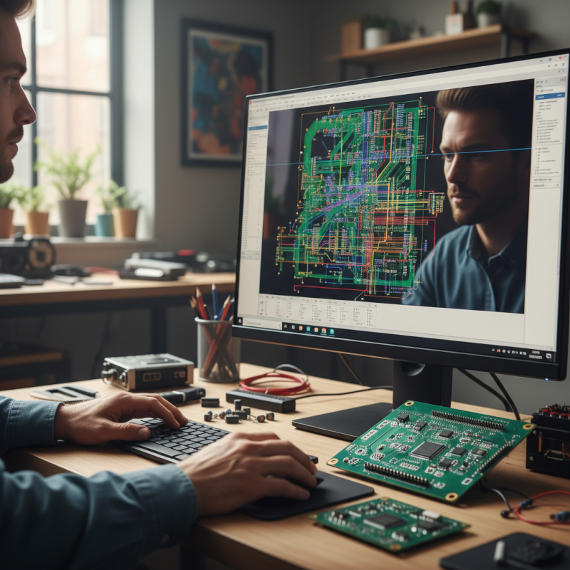
Designing printed PCB for your electronics projects can be exciting but challenging. A well-designed printed PCB can greatly impact the functionality of your device. It serves as the foundation for your electronic components, providing the necessary connections and pathways for signals to travel.

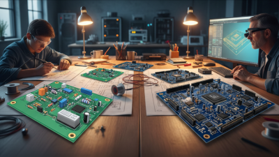
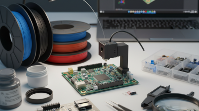
In this guide, we'll explore several key aspects of printed PCB design. From choosing the right materials to understanding layout techniques, each detail matters. Consider how your design will be manufactured and tested. Mistakes in the design phase can lead to costly errors later. Think about space and airflow, especially when components heat up.

It's essential to embrace the learning curve. Every designer faces pitfalls along the way. Reflecting on these challenges can lead to better designs in your future projects. By applying thoughtful design principles, you can create a printed PCB that not only meets your project's needs but also enhances its performance.

How to Design Printed PCB for Your Electronics Projects?

Understanding the Basics of Printed Circuit Boards (PCBs)

How to Design Printed PCB for Your Electronics Projects?

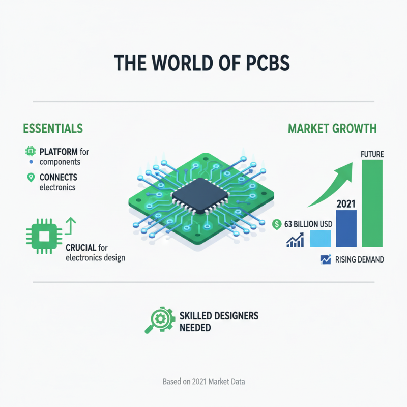
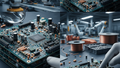
Printed Circuit Boards (PCBs) are essential for modern electronics. They provide a platform for connecting electronic components. A strong understanding of PCB design is crucial for any electronics project. In 2021, the global PCB market was valued at approximately $63 billion. This figure is expected to grow, indicating a rising demand for skilled PCB designers.

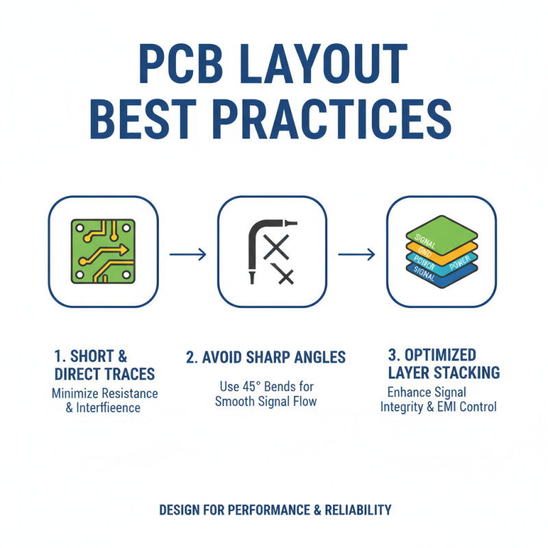
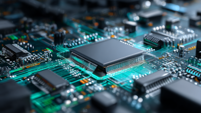
The fundamental aspect of PCBs lies in their layers. Most PCBs are made of multiple layers of material. These include copper, insulating layers, and a protective finish. The design process demands precision. Improper layout can lead to circuit failures. In fact, improper routing is one of the top reasons for PCB failure, cited in various industry reports.

Moreover, selecting appropriate materials is not always straightforward. Different applications require different substrates. For example, high-frequency circuits may need specific materials to minimize signal loss. A flawed choice here can alter the performance of the final product. Therefore, it becomes essential to research material properties and compatibility with design requirements. Proper planning and experimentation in this stage can prevent costly mistakes later.

Choosing the Right Tools and Software for PCB Design

Choosing the right tools and software for PCB design is crucial for any electronics project. You can find many options. Each has unique features and workflows. Some tools are user-friendly, while others cater to advanced needs. It's important to assess your skill level. Beginners might prefer software that offers guided tutorials. Advanced users often seek more customizable solutions.

While selecting software, consider collaboration features. Many projects require teamwork. Real-time sharing of designs can enhance productivity. However, not all tools support this. Another aspect is cost. Some software options are free, and others come with a subscription fee. Ensure the tool fits your budget. Free software may lack some features. A limited tool can add frustration during critical phases.

Don't forget about component libraries. Reliable access to parts is essential. Missing components can stall projects. Some tools have extensive libraries, while others depend on user contributions. This can lead to inconsistencies. You might spend more time troubleshooting. Reflect on the user reviews of the tools. Although feedback can guide your choice, every project is unique. Hence, personal experience is invaluable.

Steps to Create a Schematic Diagram for Your Circuit

Creating a schematic diagram is a fundamental step in designing printed PCBs. It translates your idea into a visual format. This phase is crucial because incorrect schematics can lead to failed circuits. A study by PCB design experts states that nearly 30% of projects face delays due to schematic errors.

Begin by selecting the right software for your project. Popular options can streamline this process. Draw symbols for each component. Be consistent with your placements. Ensure you're adhering to standardized conventions. Clarity is important. Misplaced components will create confusion during the layout phase.

Once your schematic is complete, review it carefully. Validate each connection and component. The average design time can take several hours, but rushing this stage often results in mistakes. It’s common to overlook simple connections, which can lead to significant issues later. Circuit misconfigurations account for up to 25% of PCB failures in the field. Proper attention to this detail can save time and effort in the long run.

Designing the PCB Layout: Best Practices and Tips

How to Design Printed PCB for Your Electronics Projects?

When designing a PCB layout, a few best practices can make a big difference. First, keep trace lengths short and direct. This minimizes resistance and reduces interference. Avoid sharp angles; instead, use 45-degree bends for smoother signal flow. Layer stacking is crucial. A good arrangement can enhance signal integrity and control electromagnetic interference.

Ground planes are essential in any PCB layout. They provide a reference point and reduce noise. However, some designers overlook them. It's easy to forget about grounding when focusing on component placement. Regularly checking for ground connections can save a lot of trouble later. Use vias wisely, but don’t overuse them. Too many can complicate the layout and increase costs.

Remember, spacing between traces is vital. It prevents unintentional short circuits. Yet, many designs are too dense, leading to problems. Testing your layout before finalizing is a must. Simulations can reveal flaws. Take time to review your layout critically. Sometimes, stepping away helps to see issues you missed initially.

Finalizing Your PCB Design for Fabrication and Assembly

Finalizing your PCB design for fabrication and assembly is crucial. Many designers overlook details that can lead to costly mistakes. According to a recent industry report, nearly 37% of PCBs are rejected due to design flaws. Achieving optimal design requires careful attention to specific factors.

Design rule checks (DRC) can help identify errors before fabrication. Use software tools that provide DRC features. Ensure traces are the correct width to handle the required current. A trace that’s too narrow can overheat and fail. Additionally, component placement matters. Parts should be easy to access for soldering and future maintenance. The layout should allow signal integrity, especially for high-frequency applications.

Thermal management is another often-neglected aspect. Poor heat dissipation can damage components. Incorporate thermal vias and heat sinks to reduce hotspots. Remember to factor in the material used for the PCB. Some materials can affect the overall performance and cost. Regularly reviewing these details can prevent delays and enhance project outcomes.