Skip to content

How to Design and Manufacture Printed Circuit Boards?

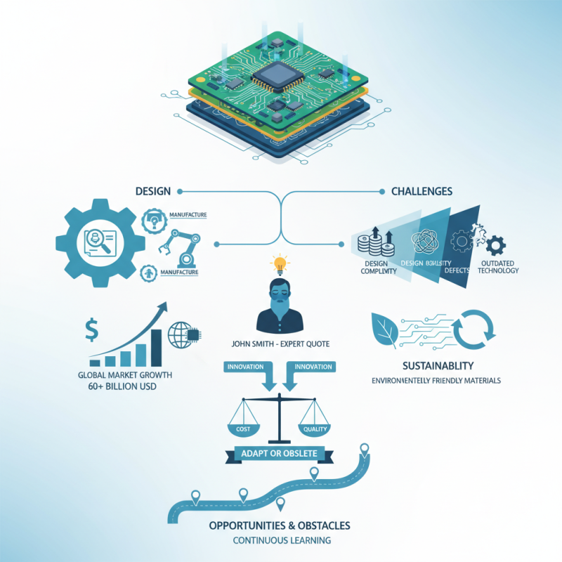
The design and manufacture of printed circuit boards (PCBs) represent an essential area within the electronics industry. The global PCB market reached a value of over $60 billion in 2022, with an expected growth rate of 4.5% annually. However, challenges persist, including increasing material costs and design complexities. As experts like John Smith, a leading figure in PCB manufacturing, state, "The future of printed circuit boards hinges on innovation and sustainability."

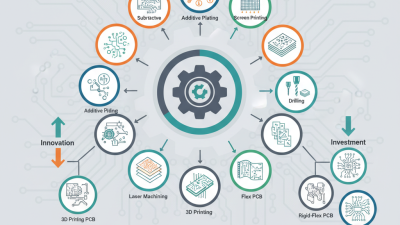
The intricacies of PCB design demand careful attention. There is a pressing need for high-quality materials that ensure performance and reliability. An average PCB factory relies heavily on advanced automated processes for efficiency. However, many manufacturers still face significant hurdles. Outdated technologies can lead to defects, which are costly to resolve. The focus must also shift towards environmentally friendly materials, as sustainability becomes a key market driver.

In the evolving landscape of PCBs, companies must adapt or risk obsolescence. The balance between cost, quality, and innovation is critical. Continuous learning and adaptation within the industry are necessary, as each design represents a unique set of challenges. The path to successfully manufacturing printed circuit boards is filled with both opportunities and obstacles.

How to Design and Manufacture Printed Circuit Boards?

Understanding the Basics of Printed Circuit Board Design

How to Design and Manufacture Printed Circuit Boards?

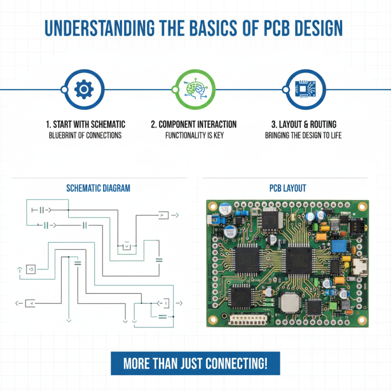
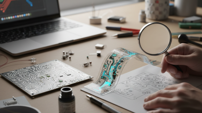
Designing printed circuit boards (PCBs) requires a solid understanding of the fundamentals. It's not just about connecting components; it's about making them work together. Start with a schematic diagram. This blueprint outlines the connections and functionality of each component. Knowing how each part interacts is crucial.

When laying out the PCB, pay attention to the placement of components. Proper spacing can reduce interference and improve performance. Use software tools to help visualize your board. These tools can catch potential errors before manufacturing begins.

**Tips**: Check for the minimum distance between traces. This can prevent unwanted short circuits. Consider using via holes wisely—they can add complexity to routing.

One common mistake is overcrowding the layout. Too many components in a small space can lead to overheating. Reflect on your design choices—are all components necessary? Streamlining can enhance efficiency. Take time to review your design multiple times. Simplifying can lead to a more effective PCB.

Selecting the Right Materials for PCB Manufacturing

Selecting the right materials for PCB manufacturing is crucial. The choice of materials affects durability, conductivity, and overall performance. Commonly used substrates include FR-4, a fiberglass epoxy laminate. It's widely favored due to its excellent insulating properties. However, its heat tolerance might not be sufficient for all applications.

Other materials, like polyimide, can withstand higher temperatures. They are preferable for flexible PCBs. Yet, polyimide can be more costly. When choosing a material, consider the specific environment your PCB will encounter. Moisture, temperature fluctuations, and mechanical stress may dictate your selection.

Consider the copper thickness used in PCBs. Thicker copper can improve current handling but complicates the manufacturing process. It's a balancing act to select the right gauge. Reflect on the potential trade-offs with each material. Sometimes, the best choice isn't the most popular one. Each project may call for unique considerations, inviting creativity in the process.

Materials Selection for PCB Manufacturing

Steps in the PCB Design Process: From Concept to Prototype

How to Design and Manufacture Printed Circuit Boards?

Designing and manufacturing printed circuit boards (PCBs) requires a structured process. The journey starts with concept development. This phase includes defining project goals and requirements. Sketching initial ideas on paper can help visualize layouts. However, many often rush through this step. Taking time here can prevent issues later.

Next comes schematic design. Using software, engineers translate concepts into detailed schematics. Each component must be specified accurately. Small errors in this stage can lead to malfunctions. Creating a library of components helps streamline this process. Often overlooked, it is vital to maintain consistency across designs.

After the schematics, PCB layout design follows. Engineers arrange components in a way that minimizes space and maximizes efficiency. Routing traces between components requires careful consideration. Many designs face challenges during this stage. Testing the layout for potential issues is crucial. If done hastily, it can cause performance setbacks. Prototyping should also include testing for signals and functionality. Each iteration brings insights for future improvements. This process, while intricate, is essential for creating reliable PCBs.

Manufacturing Techniques for High-Quality Printed Circuit Boards

Designing and manufacturing high-quality printed circuit boards (PCBs) involves several key techniques. The choice of materials is critical. Copper thickness directly impacts conductivity, and the dielectric layer affects overall performance. Selecting suitable substrates, like FR-4, is essential for durability.

When it comes to manufacturing, the process usually starts with etching. This technique removes unwanted copper, forming the circuit paths. It’s essential to control the etching time. Over-etching can lead to thin traces that may break. A common issue is inadequate cleanup after etching. Residues can cause faults.

Tips for maintaining quality include using high-resolution images of designs. Always double-check for errors in the layout before fabrication. Testing prototypes helps identify possible issues early. Consider using less common materials that might provide better results, but be aware of compatibility problems. Balancing performance with cost can be challenging, yet necessary for producing reliable PCBs.

Testing and Quality Assurance in PCB Production

Testing and quality assurance in PCB production are critical steps. After manufacturing, each PCB needs thorough testing. Simple visual inspections are often not enough. Engineers should check for shorts or open circuits. Automated Optical Inspection (AOI) can efficiently spot defects. However, even with machines, human oversight is essential. Mistakes can happen. A small error can lead to significant failures later.

Functional testing is also necessary. This involves checking each circuit's operation under real conditions. It's time-consuming but crucial for reliability. Documentation of test results should be meticulous. If a board fails, the reasons must be clear. Sometimes, guidelines are not followed properly. It’s important to reassess processes when failures occur.

Additionally, quality assurance should not end with testing. Continuous monitoring during production is vital. Feedback from testing should inform future designs. Adopting a culture of quality is essential but challenging. It requires commitment from every team member. Only then can the industry improve and reduce defects in PCB production.